
Capabilities of Diamond
Synthetic diamond made by Chemical Vapor Deposition (CVD) is a fast growing, cost effective material. Delivering the superior properties of diamond in larger sizes, at a lower cost and with increased post- processing capabilities; CVD Diamond has replaced less effective materials in existing industries and become the chosen material for challenging next generation applications.
Thermal conductivity can be tailored to Your Needs:
- Low – black diamond 700-800 W/mK
- Medium – opaque diamond 900-1000 W/mK
- High – optically clear diamond 1700-1800 W/mK
Customized sizes for unique applications:
Diamond growth can be on 2, 2.5 and 3″ wafers. Free standing diamond can be grown to thicknesses ranging from 80 µm to 1 mm. Specific diameters and geometries can be laser cut to produce custom parts for unique applications. Diamond can be grown as thin as 30 nm directly on Si as a membrane or supported by a lattice structure.
Standard Thicknesses:
- 150 µm
- 300 µm
- 500 µm
Post-Processing Techniques for Specific Requirements
Diamond polishing equipment can make the surface finish of materials highly smooth, less than 10 nm PV if required. Additional post-processing capabilities include metalization for bonding, mounting to a flange for vacuum and pressure applications and brazing.
Strong, Affordable Material for a Variety of Uses
Whether it’s thermal management, optical transmission or thin diamond applications, CVD diamond has become the optimal material of choice. CVD diamond is presently used in a variety of industries including defense, electronics, homeland security and medical.
Diamond UV and X-Ray Detectors, Gamma (y) Ray Radiometers,
Charged Particle Detectors and Bio and Chemical Sensors
 HIGH purity synthetic CVD Diamond presents unique characteristics that make it an excellent material for radiation detection. Diamond can detect any kind of radiation that is more energetic than its band gap of 5.5 eV, e.g., deep UV photons, x-rays, gamma rays, charged particles and neutrons with a dynamic range in energies spanning from 5.5 eV up to GeV of cosmic rays. Because of its radiation hardness it needs no frequent replacements, its high mobility for both electrons and holes equates into a very fast response (rise time < 100 ps). It can be operated at room temperature with no need for cooling. It has a resistivity several orders of magnitude greater than silicon, an extremely low leakage current and a thermal conductivity better than copper. More on radiation detection.
Technical Notes:
Optical Transmission
Diamond has an exceptionally high transmission over a very broad range of wavelengths (Diamond Optics Transmission Properties). It is extremely hard and chemically inert; making CVD diamond the optimal choice in applications demanding higher power, larger area, resistance to hazardous materials or greater strength. EOC offers optical grade diamond films in a variety of thickness and cut to various geometries. Diamond’s exceptional properties provide benefits in a variety applications:
- High Energy Research
- X-ray
- Multi-wavelength Spectroscopy
- Infrared and Terahertz
- Microwave
- High Power Laser
- Monochromators
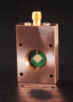
Wedged windows are available to minimize interference oscillations. Mounted windows in flanges for vacuum application are also available.
Free standing diamond can be grown to thicknesses ranging from 80 µm to 1 mm and are available in up to 3″ diameter. Specific diameters and geometries can be laser cut to produce custom parts for unique applications. Standard thicknesses are 150 µm, 300 µm and 500 µm. and can be processed with an anti-reflective coating.
Thermal Management
Use the ultra high thermal conductivity of diamond for temperature critical packages. Higher power in smaller devices, and the integration of these to other devices present heat dissipation challenges. High thermal heat flux significantly impacts performance and reliability. The unsurpassed thermal conductivity of diamond and its high electrical resistivity, allow for increased microprocessor frequency, higher output power, smaller parts and longer lifetimes.
Diamond has thermal conductivity five times that of copper and is an electrical insulator, making for a perfect heat sink. CVD Diamond has all of the properties of single crystal diamond without many of the size and shape limitations. CVD Diamond is being used in the following applications:
- RF Power Devices
- Power Semiconductors
- High Speed Processors
- Radar Amplifiers
- High powered laser diode arrays
- LEDs
- Multi chip power module packages
- Flip chip
Diamond also has a low density for lighter weight applications of aircraft and space craft electronic systems, notebook computers and other mobile devices.
Thermal Conductivity
CVD Diamond has exceptional thermal conductivity and diffusivity. EOC offers thermal conductivities tailored to the cost/performance requirement of our customers, including:
- Low – black diamond 700-800 w/mK
- Medium – opaque diamond 900-1000 w/mK
- High – optically clear diamond 1700-1800 w/mK for the most difficult heat problems
Superior Properties for Next Generation Applications
Diamond’s tensile strength, beam resistance, low noise, fast response and transmission across a variety of wave lengths, make it a superior material for a variety of challenging high energy research applications. Single crystal and CVD diamond can be configured for the following applications:
- Particle detectors – UV, X-ray and electron beam
- Beam diagnostics and positioning
- Stripper foils
- Synchrotrons
Thin Diamond Applications
Used in high energy, x-ray and thermal isolation applications
Manufacturing innovations have led to cost effective solutions for our clients’ next generation applications. EOC offers foils, films, windows and detectors which out-last and out-perform alternative materials. Thin diamond products are available in 300nm to 5μm thickness. We offer both nano and microcrystalline diamond films, tailored to your application requirements.
Single Crystal Diamond
Single Crystal Diamond parts are manufactured from all types of diamond, all crystallographic orientations, and a wide range of dimensions and geometries. Single Crystal Diamond offers outstanding properties for the most challenging applications. Unique windows, targets, diamond slabs, and other parts customized to fit our client’s requirements are available. Diamond is highly transparent over a wide range of wavelengths, including x-ray, visible, IR, microwave, terahertz and more.
| Common Sizes | Standard Thickness | Orientations |
|---|---|---|
| 3 mm dia | 20 µm | <110> |
| 3 x 3 mm dia | 100 µm | <100> |
| 4 x 4 mm dia | 300 µm | <111> |
| 500 µm |
Diamond is used as windows in flow chamber accessories for IR spectrometers. Its biological inertness makes it an ideal substrate for cell growth studies. A relatively constant index of refraction makes for minimal dispersion and superior transmission across the mid- IR and visual spectral wavelengths allowing for chemical imaging of living cells. Its chemical inertness makes the diamond easily cleaned between studies, too. The flow chamber made with sub micrometer thick diamond allows for a slim profile which minimizes working distances.
Single crystal diamond used for Failure Analysis, IREM
Thin diamond windows are finding applications in semiconductor failure analysis. Tougher and more durable than sapphire, diamond is preferred in sensitive magnetic microscopes that probe fields in operating ICs. IREM – InfraRed Emission Microscopy – also utilizes diamond as an interface between an operating IC and the infrared detector. Diamond’s unsurpassed thermal conductivity together with its exceptional IR transmission help in the detection of hot spots during IC development and troubleshooting. The superior strength of diamond allows for relatively thin window dimensions minimizing both cost and absorption.
Spectroscopy
Single crystal diamond used for sample surface in FTIR accessories
Diamond is widely used as the sample surface in FTIR accessories. Its mechanical strength permits significant forces to be used insuring intimate contact with the sample. Low absorbance gives great throughput improving the instrument’s sensitivity across a broad spectral band. Diamond’s chemical and abrasion resistance makes it impervious to thorough cleaning and especially valuable in situations with abrasive and/or corrosive chemicals are analyzed.
Beam Line Components
Single crystal diamond used for x-ray, laser, and reactive ion beam line components
The unsurpassed thermal conductivity of diamond and its low absorbance makes it an ideal material for beamline components, especially as the power of these x-ray, laser and reactive ion beamlines continue to increase. Whether your beam is photons, protons or heavier ions, diamond will minimize beam losses and efficiently conduct energy that is lost to the cooling systems. Diamond is increasingly used for output coupling, filtering, beamsplitting, beam detection, position monitoring and sample holding. Diamond is often brazed into flanges to withstand pressure differences and can be thin enough to minimize absorption of x-rays.
Diamond Targets
Due to its low Z and high density, diamond has found interest as a target material for high power, short pulse length lasers. Its high density leads to a high shock velocity, so that a high energy yield can be delivered to a sample though a reasonably thin diamond holder. Its low Z leads to low x-ray generation, minimizing noise in downstream analysis equipment. The carbon ion beams that result from this laser bombardment have potential uses in fusion power development, ion cancer therapy and material studies.
Customized Solutions
EOC provides CVD Diamond products for applications from the most common to the most sophisticated, including components for materials research and a virtually limitless variety of applications. We can meet our clients’ specialized needs by delivering a wide range of solutions from a 50 micron in diameter diamond coated tungsten carbide cutting plate to a customized nozzle for highly corrosive liquids.
Cutting Tools
CVD diamond is used extensively for precision cutting tools, wear components and scalpels. Extend tool life and enhance tool performance with customized solutions. For more information about our customized tool products contact EOC.
Detectors
Research continues in the development of CVD diamond as a radiation detector for medical and high energy physics applications. Major fields of application include medical dositry, neutron detectors, UV laser systems and X-ray and gamma detection.
Silicon on Diamond
Silicon on diamond (SOD) is achieved by joining a thin single crystalline Si device layer to a thin CVD diamond layer. Diamond replaces the silicon dioxide in the silicon on insulator structure and serves as an electrical insulator, heat spreader and support substrate. Like silicon dioxide, diamond is a good electrical insulator with the added advantage of diamond’s far superior thermal conductivity. As a result, SOD can sustain more than 10 times higher power than SOI, permitting more than 3-fold greater integration density of circuits. Devices such as MOSFETS, Bipolar transistors, JFETS and diodes can be fabricated in the recrystallized silicon that sits on top of the diamond film.
Exceptional Properties, Expert Support
EOC can provide more than just material to your challenging applications. We pride ourselves on the creative collaboration and innovative solutions we offer clients. Our extensive knowledge of diamond and years of practical application have allowed us to tailor fit our materials to your particular needs. We assist our clients in solving the challenges of cutting-edge research where no other material will suffice.
Services
Grinding and Polishing Services
Due to its extreme hardness, wear resistance and low coefficient of friction, diamond can be a challenge to polish. The roughness on a 500 µm CVD diamond wafer may be as much as 50 µm before polishing but specialized equipment can polish diamond to a very smooth, mirror surface resulting in a Peak-to-Valley (PV) roughness of less than 10 nm on both sides. Call or email us today to discuss your needs and a practical way of achieving your goals.
Laser Sawing and Scribing
Use our laser capability in conjunction with our other processes to produce finished parts from your CVD diamond raw material. You’ll find our engineers knowledgeable regarding what is possible and how we can work together most efficiently and economically. We work hard to keep our services quick and inexpensive, too. Historically, a Q-switched Nd:YAG laser has been used for sawing diamond, whether single crystal or CVD. The beam delivery optics and the part being cut are moved relative to one another in order to cut parts of specific geometry. The resolution of the moving stages, specifications of the delivery optics, and performance of the laser determine the amount of material removed, quality of the cut and minimum tolerances that can be held. We can cut samples over 1 mm thick and hold dimensional tolerances to +/- 10 microns (.0005 in.) The computer-controlled stages allow a wide variety of shapes to be cut; we’ve even done crescents and stars. Small and large jobs can be accomplished quickly and economically with this system. Laser cutting also works well for scribing and cleaving thin diamond layers on silicon wafers.
Metalization
Metalization can also be used in applications when diamond is a new addition to an existing process. Coating the diamond with metal can permit low temperature bonding of diamond in the semiconductor, optoelectronic and tool-making industries. Diamond metalization schemes usually involve three different metals. The first, closest to the diamond, is a carbide-former such as titanium, tungsten or chromium. These metals make a chemical bond with the diamond to insure adhesion of the metalization. A diffusion-barrier is then applied, typically palladium or platinum. Finally the layer required for the process is added. Gold or silver are usually used to prepare the diamond for brazing, eutectic bonding or other attachment techniques. Our standard metalization scheme is:
- Titanium – 1,000A
- Platinum – 1,000A
- Gold – 10,000A
Vacuum Brazing
Active brazes can be used in a variety of vacuum apparatus for brazing diamond parts and shapes to holders of various designs. Brazing of diamond to other materials is always done in a vacuum or inert atmosphere to avoid oxidation. Examples of our vacuum brazing include:
- Bonding single crystal or CVD diamond parts to tool shanks and inserts
- Vacuum-tight joints between diamond windows and vacuum fittings
- CVD diamond film applied to tungsten carbide backing (to allow brazing in air to tool shanks)
- Diamond slabs sintered between powder metal blanks